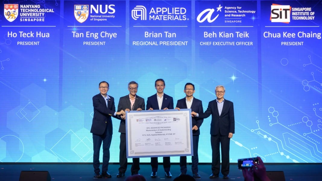
Applied Materials, a leader in semiconductor innovation, has announced the expansion of its global EPIC innovation platform, introducing a new collaboration model designed to fast-track the development and commercialisation of advanced chip packaging technologies. The company gathered more than two dozen top semiconductor research and development (R&D) leaders at a summit in Singapore, with the aim of fostering alliances between equipment manufacturers, material providers, device companies, and research institutes. The goal of the initiative is to accelerate the creation of technologies that will power the next generation of energy-efficient computing.
The rise of connected devices and the increasing demand for artificial intelligence (AI) have significantly impacted the semiconductor industry. However, alongside these growth opportunities, the industry faces challenges, particularly the rising energy consumption due to the immense compute power needed to support AI’s rapid development. As a result, chipmakers and system designers are turning to advanced packaging technologies and the heterogeneous integration of multiple chips to achieve better energy efficiency.
The role of advanced packaging in driving AI innovation
“Advanced packaging is paramount to the semiconductor roadmap for enabling sustainable progress in the AI era,” said Dr. Prabu Raja, President of the Semiconductor Products Group at Applied Materials. He emphasised that the summit brought together leaders from some of the most innovative organisations to discuss how advanced chip packaging can improve performance-per-watt. With its EPIC Advanced Packaging strategy, Applied Materials is aiming to help chipmakers accelerate the journey from concept to the commercialisation of cutting-edge technologies.
Currently, the most advanced AI chips rely on multiple advanced packaging techniques, such as micro-bumps, through-silicon vias (TSVs), and silicon interposers. The industry is now working on developing a new set of packaging technologies that will increase interconnect density and bandwidth to unlock AI’s full potential. However, the development of these new technologies involves multiple simultaneous innovations, and the pace of product introductions is increasing, adding complexity and risk to chipmaker roadmaps.
The growing complexity of packaging architectures and the challenge of navigating various solution paths require more collaboration across the semiconductor ecosystem. Applied Materials aims to address this need through its EPIC Advanced Packaging initiative, which promotes co-innovation among partners and shifts the approach to developing and commercialising foundational packaging technologies.
EPIC Advanced Packaging’s global network of innovation centres
The new EPIC Advanced Packaging initiative will leverage Applied Materials’ global network of innovation centres to give chipmakers and system designers early access to the next-generation technologies and equipment. The aim is to provide a platform for deeper collaboration with suppliers and academic institutions, strengthening the pipeline from laboratory research to full-scale production. Additionally, the initiative seeks to support the development of future semiconductor talent by encouraging more engagement with university partners.
This collaboration is an extension of Applied Materials’ EPIC platform, which launched in May 2023 with the establishment of the EPIC Center in Silicon Valley. While the EPIC Center focuses on equipment and process technologies for creating transistors and wiring on individual chips, the EPIC Advanced Packaging expansion focuses on the development of technologies that connect multiple chips within a computing system, enhancing overall system performance.
Companies and institutes involved in the summit
The summit saw participation from leading semiconductor companies, including Absolics, Advantest, AMD, Amkor, Intel, Broadcom, Micron, Samsung, SK hynix, and TSMC, as well as key research institutions such as A*STAR’s Institute of Microelectronics, the Singapore Economic Development Board (EDB), and the National University of Singapore (NUS).
Applied Materials’ initiative highlights the growing importance of collaborative efforts within the semiconductor industry to address the challenges posed by the rapid development of AI technologies and the increasing demand for energy-efficient solutions. The launch of EPIC Advanced Packaging represents a significant step towards realising the potential of next-generation computing systems.


